Method and Apparatus for Modeling Electromagnetic Fields using Hermite Finite Elements
In optoelectronic device development, the design and prototyping process can be costly and time consuming. To mitigate costs, computerized devices can be utilized during the design process to simulate the operation of the electronic device prior to the construction of a physical prototype. For example, conventional computerized devices can be configured to utilize mathematical models to represent or approximate the electronic device, such as an electronic package or a multi-layer printed circuit board (PCB), and can simulate the response of the device during operation.
With certain electronic devices, such as antennae or integrated circuits, the presence of electromagnetic fields generated by the device can affect device operation. For example, with the ongoing development of integrated circuit technology, under the principle of Moore’s law, the number of transistors in an integrated circuit will increase over time. The increase in the number of transistors can affect the presence of electromagnetic fields and can increase unwanted crosstalk. The cross-talk, in turn, can interfere with integrated circuit signal propagation. Therefore, in order to identify and mitigate the potential effects of the electromagnetic fields on electronic devices, such as integrated circuits, before physical prototypes are constructed, device designers should also utilize computerized devices to simulate the presence of the electromagnetic fields within the electronic devices.
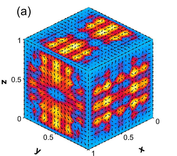
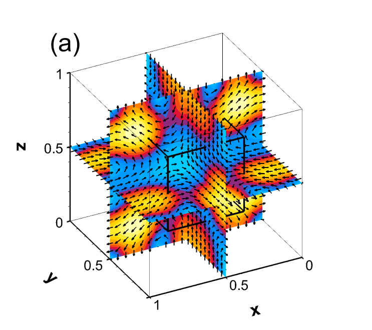
The method includes receiving, by the modeling apparatus, geometric design criteria and material property criteria for the electronic component. The method includes defining, by the modeling apparatus, a set of finite elements representing the electronic component based upon the geometric design and material property criteria. The method includes representing, by the modeling application, an electromagnetic field of each finite element by a Hermite interpolation polynomial; imposing, by the modeling application, a divergence-free condition at each node of each finite element to define the electromagnetic field at each node; and based upon application of the Hermite interpolation polynomial and divergent free condition, displaying, by the modeling application, a model of the electromagnetic behavior and working characteristics of the electronic component on a display.
By providing a node-based Hermite finite element representation, the modeling device provides consistency in the direction of fields at the vertices of elements and, hence, is well suited to model transport problems such as electron microscope design and particle accelerators where the particles are driven by microwave fields. Accordingly, the modeling device can provide multiscale calculations with minimal computational costs, which is not feasible within currently prevalent Vector finite element methods that are used in most of the software packages, due to their lack of unique directionality for fields at shared nodes in the finite element mesh.
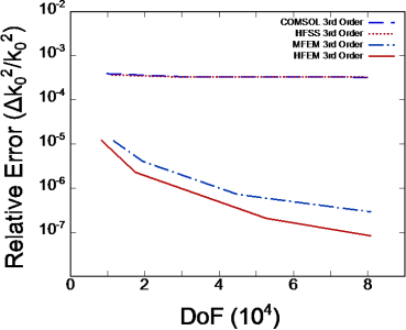
- Our method is shown to produce higher accuracy with lesser computational cost while compared to the electromagnetic simulations implemented in popular software packages such as COMSOL (produced by COMSOL Inc.), HFSS (produced by ANSYS, Inc.), and MFEM (produced by CASC, LLNL).
- Edge-based vector finite element methods used in other software are ineffective in modeling multi-physics problems which will involve quantum mechanical and electrodynamic aspects in tandem, such as designing cavity lasers. In such instances, independent numerical treatments are needed to obtain wave functions and electromagnetic (EM) fields.
- Unlike our approach, the conventional methods with vector basis functions produce ambiguous vector field description. When they are employed in further applications, such as determination of electron trajectories in accelerators or in high power vacuum tube design, these regions around vertices inject uncertainties in the charged particle trajectories.


Key Features/Benefits
- The method can obtain high spatial resolution of the electromagnetic field while mitigating the effects of computational scaling and discretization errors in both two and three dimensions.
- The use of Hermite interpolation polynomials improves the operation of the modeling device relative to conventional computerized devices by reducing the amount of time necessary to generate a model of an electromagnetic field.
- The modeling device can provide results having several orders of higher accuracy and smoother representation of the electromagnetic fields with fewer elements in an optoelectronic device than those needed in the presently prevalent 3D implementations of commercial softwares.
- Due to the consistency in field directions, it can be used to study transport problems such as electron microscope design and particle accelerators where the particles are driven by microwave fields. Accordingly, the modeling device can provide multiscale calculations with minimal computational costs, which is not feasible with Vector finite element methods due to the lack of unique directionality for fields at shared nodes in the finite element mesh.
- The ability to reproduce smooth variational solutions for the fields will allow a coarsely discretized full-wave Maxwell solver to seamlessly couple to other solvers for physically small features, such as small gate geometries, quantum wells and dots, or plasmonic structures which are all deeply subwavelength.