Our invention impacts on the design-modeling-manufacturing cycle of nano-scale chips for wearable electronics, quantum information technology, and spintronics devices. To design meso- and nano-scale structures, a fully variational method for scattering is appropriate to account for geometrical complexities and defect and/or impurity distributions present in the manufactured material. In one embodiment, the nano-scale quantum transport design and manufacturing system includes a computerized device, such as a design component, configured to receive design criteria and wave propagation criteria from a manufacturer for a given electronic component, such as a waveguide.
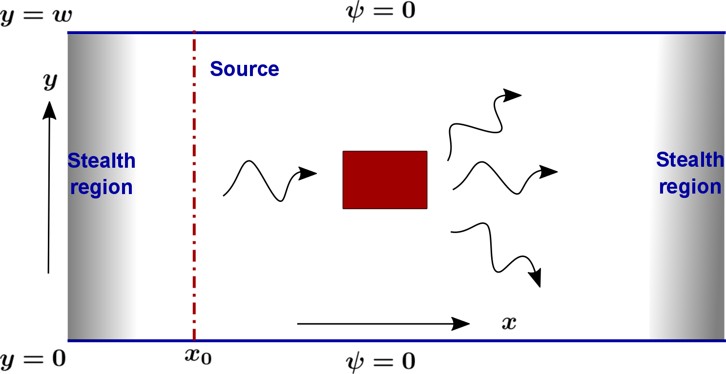
Conventional waveguide design typically utilize asymptotic boundary conditions with globally defined wavefunctions. Such global approaches are not applicable to domains limited to meso- and nano-scale structures since they cannot capture the presence and effects of near field solutions as they obtain the solutions in the asymptotic limit. For example, in a typical quantum scattering problems, partial wave analysis and Born approximations can be applied to obtain approximate far field solutions. However, in finite nanoscale systems, these analysis methods cannot be applied since the meso- and nano-scale geometry itself is confined.
The design component is configured to apply modeling criteria, such as a finite element method (FEM), to the design criteria to generate manufacturing data which comports with the wave propagation criteria received from the manufacturer. The nano-scale quantum transport design and manufacturing system can also include a manufacturing component configured to receive manufacturing data generated by the computerized device and to produce a meso- and nano-scale waveguide as required by the manufacturer.
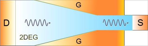
During operation, and in response to receiving geometric boundary and electrical property information as design criteria, the design component is configured to define the boundaries of a waveguide and to apply the modeling criteria to the design criteria to generate a waveguide model. For example, assume the case where the design component receives geometric boundary information which requires a tapered waveguide and electrical property information requiring a particular resistivity of the waveguide. Based upon this design criteria, the design component is configured to define a waveguide model as having tapered boundaries and is configured to provide inclusions within the waveguide boundaries to provide the prescribed resistance in the waveguide model. Such tapered waveguide geometry can be used as a current rectifier in electron transport circuits.
The resulting meso- and nano-scale waveguides can be utilized in a variety of applications, such as in wearable electronics, spintronics, quantum information, and computing technology.
- The design component is configured to provide more accurate results compared to transfer matrix, S-matrix, and boundary element methods all of which have serious discretization errors.
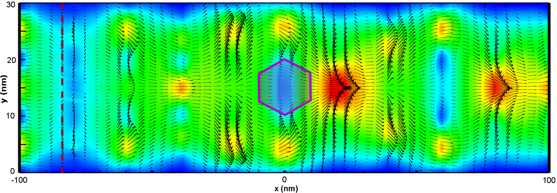
- Contribution from evanescent modes are lost when conventional asymptotic methods are used. The design component is able to capture evanescent mode contributions through a novel sources and absorbers method.