
In physics, scattering theory provides the basis for understanding how waves and particles scatter when they encounter material objects. Two papers published consecutively in the Journal of Applied Physics this spring have the potential to alter and simplify the way the standard calculations for scattering are carried out in quantum mechanics.
“We have shown that certain assumptions that have been built into scattering theory are unnecessary and limiting in their outcomes,” says L. Ramdas Ram-Mohan, professor of physics and director of the Center for Computational Nanoscience, who co-authored the two papers with PhD candidate Sathwik Bharadwaj. “Our method provides new benchmarks with regard to what the new results are. We have done this in 2D scattering, but we are able to investigate 3D scattering problems with the same formalism.”
In conventional scattering theory, sources and observers (or detectors) are considered to be at a considerable distance from the scattering centers. But such approaches are not applicable to domains limited to meso- and nano-scale structures as they cannot capture the presence and effects of near field solutions.
For example, in typical quantum scattering problems, partial wave analysis and Born approximations can be applied to obtain approximate far-field solutions. However, in finite nanoscale systems, these methods of analysis can’t be applied since the meso- and nano-scale geometry itself is confining.
In the Journal of Applied Physics papers, Bharadwaj and Ram-Mohan offer a non-asymptotic, variational description for quantum scattering theory that avoids the need to go to great distances. Their approach involves the addition of absorbers that smoothly absorb waves with no reflections and an antenna or source close to the absorbers. “It’s like having a flashlight that you can switch on, not at a great distance, but close by,” Ram-Mohan says. “This makes a big difference.”
The authors used this approach to sources and absorbers to study transport properties of electrons in quantum waveguides. They introduced absorbing regions, which they also call “stealth regions,” to enclose the active scattering region, providing a unique way of simplifying and applying boundary conditions.

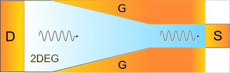
Figure 1. Split-gate geometry for a tapered waveguide
“Once we put in these absorbing regions or stealth regions, waves produced by the antenna are scattered and absorbed away,” Ram-Mohan says. “This makes life extremely easy and increases the accuracy of the method. We are able to do many, many calculations that most other people have hesitated to do, such as an actual scattering quantum dot within a waveguide. Few attempted it because it was a complicated calculation.”
Bharadwaj and Ram-Mohan report for the first time in these two articles the results on transport in tapered waveguides, and demonstrate a novel way of manufacturing nano-scale current rectifiers. This configuration is readily achievable using split-gate geometry on semiconductor inversion layers.
“Tapered waveguides are hard to solve, and we find that when you pass the current from one way, from the narrow side up, then all the possible current will go through. But when you come back the other way, unless you are about the height in the energy associated with the outgoing waved for the narrow channel, you will get reflected waves. So this is basically a rectifier, which can take current in one way but not the other way. This is the kind of thing that could be put in wearable electronics, for example, because we could construct it at the nano-scale. We have applied for a provisional patent for this proposed device.”

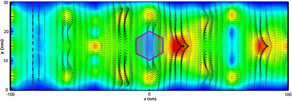
Figure 2. Current flowing through a quantum waveguide with a scattering center
They also demonstrate that quantum dots or attractive impurity potentials embedded in the interior of a waveguide provide means for enhancing the thermo-electric energy conversion efficiency beyond the presently assumed limits. “We are able to show that limitations that people thought exist with regard to the thermoelectric effect are, in fact, artificial limitations,” Ram-Mohan says. “We can actually improve upon that in a very interesting and important way.”
The nano-scale quantum transport design and manufacturing system envisaged by the authors shows a new way of simulating the ubiquitous phenomenon of scattering, and is applicable to optics, acoustics, and quantum mechanics, they note.
“I have been thinking about this since 1995,” says Ram-Mohan, who is celebrating his 40th year at WPI and his 50th year in research, “but things came into proper convergence because of the work of some undergraduates completing MQPs and the contributions of Sathwik, who has been the mainstay with regard to these two papers.”
The Journal of Applied Physics papers:
1. Electron scattering in quantum waveguides with sources and absorbers. I. Theoretical formalism, Sathwik Bharadwaj and L. R. Ram-Mohan, Journal of Applied Physics 125, 164306 (2019).
2. Electron scattering in quantum waveguides with sources and absorbers. II. Applications, Sathwik Bharadwaj and L. R. Ram-Mohan, Journal of Applied Physics 125, 164307 (2019).